NXP公司的TDF8553是I2C总线控制的 4x50W功率放大器和多个电压稳压器. TDF8553具有四个完整的采用BCDMOS技术的音频功率放大器,I2C总线用来诊断每个放大器和连接的扬声器的信息,差分模式的增益20dB,放大器模式增益为26dB. TDF8553还具有六种输出的电压稳压器,可给微控制器,显示器,音频处理器,调谐器,总线,机械数字和驱动供电,采用I2C控制. TDF8553主要应用汽车无线电和CD/MD播放器中的升压放大和电压稳压.本文介绍了TDF8553放大器和稳压器的主要特性,方框图以及测试和应用电路图及其PCB元件布局图.
TDF8553J:I2C-bus controlled 4x 50 Watt power amplifier and multiple voltage regulator
Amplifiers
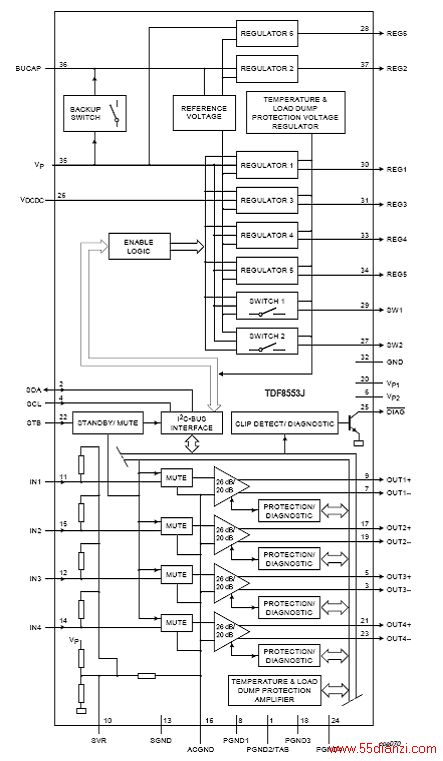
The TDF8553 has a complementary quad audio power amplifier that uses BCDMOS technology. It contains four amplifiers configured in Bridge Tied Load (BTL) to drive speakers for front and rear left and right channels. The I2C-bus allows diagnostic information of each amplifier and its speaker to be read separately. Both front and both rear channel amplifiers can be configured independently in line driver mode with a gain of 20 dB (differential output) or amplifier mode with a gain of 26 dB (BTL output).
Voltage regulators
The TDF8553 has a multiple output voltage regulator with two power switches.
The voltage regulator contains the following:
Four switchable regulators and two standby regulators
Two power switches with loss-of-ground protection and surge protection
Second supply pin to reduce dissipation by means of an external DC-to-DC converter
TDF8553主要特性:
Amplifiers
I2C-bus control
Can drive a 2 load with a battery voltage of up to 16 V and a 4load with a battery voltage of up to 18 V
DC load detection, open, short and present
AC load (tweeter) detection
Programmable clip detect; 1 % or 4 %
Programmable thermal protection pre-warning
Independent short-circuit protection per channel
Selectable line driver (20 dB) and amplifier mode (26 dB)
Loss-of-ground and open VP safe
All outputs protected from short-circuit to ground, to VP or across the load
All pins protected from short-circuit to ground
Soft thermal-clipping to prevent audio holes
Low battery detection
Voltage regulators
I2C-bus control
Good stability for any regulator with almost any output capacitor value
Six voltage regulators (microcontroller, display, audio processor, tuner, bus, mechanical digital and drive)
Selectable output voltages for regulators 1, 4 and 5
Low dropout voltage PNP output stages
High supply voltage ripple rejection
Low noise for all regulators
Two power switches (antenna switch and amplifier switch)
Standby regulators 2 and 6 (microcontroller and bus supply) operational during load dump and thermal shut-down
Low standby quiescent current (only regulators 2 and 6 operational)
Second supply pin for connecting optional external DC-to-DC converter to reduce internal dissipation
Backup functionality for regulator 2
Protection
If connection to the battery voltage is reversed, all regulator voltages will be zero
Able to withstand output voltages up to 18 V (supply line may be short-circuited)
Thermal protection to avoid thermal breakdown
Load-dump protection
Regulator outputs protected from DC short-circuit to ground or to supply voltage
All regulators protected by foldback current limiting
Power switches protected from loss-of-ground and surge conditions
TDF8553主要应用:
Boost amplifier and voltage regulator for car radios and CD/MD players
图1.TDF8553方框图
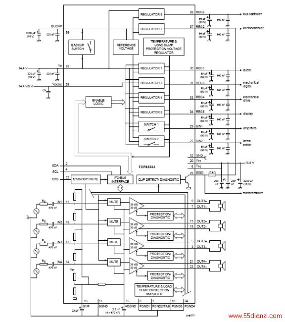
图2.TDF8553J测试和应用电路图
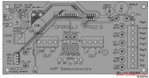
图3. TDF8553J测试和应用电路元件布局图
本文关键字:暂无联系方式电工文摘,电工技术 - 电工文摘