NXP ISP1705高速USB评估方案
点击数:7233 次 录入时间:03-04 11:59:32 整理:http://www.55dianzi.com 电子技术
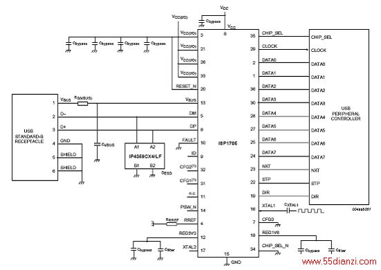
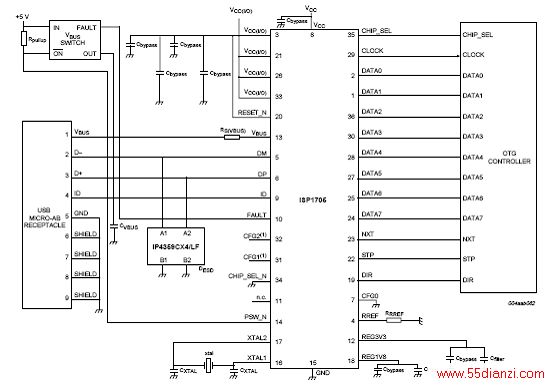
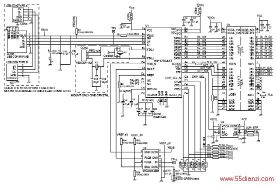
NXP公司的ISP1705是高速USB收发器,完全兼容USB 2.0 Rev.1.3与ULPI Rev.1.1标准. ISP1705能以高速(480Mbps),全速(12Mbps)和低速(1.5Mbps)等模式发送和接收USB数据,有最低的引脚数,非常适合用在便携式电子设备如手机,数码相机,数码摄像机,PDA和数字音频播放器等.本文介绍了ISP1705的主要性能,方框图,以及用作外设时的应用电路图, 在OTG 应用时的电路图与用作主机时的应用电路图.本文还介绍了ISP1705评估板方框图和详细的电路图.
The ISP1705 is a UTMI+ Low Pin Interface (ULPI) Hi-Speed Universal Serial Bus (USB) transceiver that is fully compliant with Universal Serial Bus Specification Rev. 2.0, On-The-Go Supplement to the USB 2.0 Specification Rev. 1.3 and UTMI+ Low Pin Interface (ULPI) Specification Rev. 1.1.
The ISP1705 can transmit and receive USB data at high speed (480 Mbit/s), full speed (12 Mbit/s) and low speed (1.5 Mbit/s), and provides a pin-optimized, physical layer front-end attachment to the USB host, peripheral or OTG controller with Single Data Rate (SDR) or Dual Data Rate (DDR) ULPI link. The ISP1705 can transparently transmit and receive UART signaling.
It is ideal for use in portable electronic devices, such as mobile phones, digital still cameras, digital video cameras, Personal Digital Assistants (PDAs) and digital audio players. It allows USB Application-Specific Integrated Circuits (ASICs), Programmable Logic Devices (PLDs) or any system chip set to interface with the physical layer of the USB through an 8-pin (DDR) or 12-pin (SDR) interface.
The ISP1705 can interface to devices with digital I/O voltages in the range of 3.0 V to 3.6 V. The ISP1705 is available in HVQFN36 and TFBGA36 packages.
ISP1705主要特性:
Fully complies with:
USB: Universal Serial Bus Specification Rev. 2.0
OTG: On-The-Go Supplement to the USB 2.0 Specification Rev. 1.3
ULPI: UTMI+ Low Pin Interface (ULPI) Specification Rev. 1.1
Interfaces to USB host, peripheral or OTG cores; optimized for portable devices or
system ASICs with built-in ULPI link
Complete Hi-Speed USB physical front-end solution that supports high speed
(480 Mbit/s), full speed (12 Mbit/s) and low speed (1.5 Mbit/s)
Integrated 45
10 % high-speed termination resistors, 1.5 k
5 % full-speed
device pull-up resistor, and 15 k
5 % host termination resistors
Integrated parallel-to-serial and serial-to-parallel converters to transmit and receive
USB clock and data recovery to receive USB data up to 500 ppm
Insertion of stuff bits during transmit and discarding of stuff bits during receive
Non-Return-to-Zero Inverted (NRZI) encoding and decoding
Supports bus reset, suspend, resume and high-speed detection handshake
Complete USB OTG physical front-end that supports Host Negotiation Protocol (HNP)
and Session Request Protocol (SRP)
Supports external charge pump or external VBUS power switch
Complete control over USB termination resistors
Data line and VBUS pulsing session request methods
Integrated VBUS voltage comparators
Integrated cable (ID) detector
Flexible system integration and very low power consumption, optimized for portable
devices
3.0 V to 4.5 V supply voltage input range
Internal voltage regulator supplies 2.7 V or 3.3 V and 1.8 V
Supports interfacing I/O voltage of 3.0 V to 3.6 V; separate I/O voltage supply pins
minimize crosstalk
Power down internal regulators in Power-down mode when VCC(I/O) is not present
or when the chip is not selected
Typical operating current of 13 mA to 32 mA, depending on the USB speed and bus utilization
Typical current consumption ICC is 70 A in suspend mode and 0.5 A in
Power-down mode
3-state ULPI interface by the CHIP_SEL or CHIP_SEL_N pin, allowing bus reuse by other applications
Highly optimized ULPI compliant
60 MHz, 8-pin or 12-pin interface between the core and the transceiver, including a
4-bit DDR bus or an 8-bit SDR bus
DDR or SDR interface selectable by pin
Supports 60 MHz output clock configuration
Integrated Phase-Locked Loop (PLL) supporting input clock frequencies of 13 MHz, 19.2 MHz, 24 MHz or 26 MHz
Crystal or clock frequency selectable by pin
Fully programmable ULPI-compliant register set
3-pin or 6-pin full-speed or low-speed serial mode
Internal Power-On Reset (POR) circuit
UART interface:
Supports transparent UART signaling on DP and DM pins for the UART accessory
application
2.7 V UART signaling on DP and DM pins
Entering UART mode by register setting
Exiting UART mode by asserting STP or by toggling the CHIP_SEL or CHIP_SEL_N pin
Full industrial grade operating temperature range from 40度to +85度ESD compliance:
JESD22-A114D 2 kV contact Human Body Model (HBM)
JESD22-A115-A 200 V Machine Model (MM)
JESD22-C101-C 500 V Charged Device Model (CDM)
IEC 61000-4-2 8 kV contact on the DP and DM pins

图1.ISP1705方框图

图2.ISP1705用作外设时的应用电路图

图3.ISP1705在OTG 应用电路图

图4.ISP1705作主机应用电路图
ISP1705AET评估板
The ISP1705AET evaluation (eval) kit allows system designers to evaluate the functions
and features of the ISP1705AET. The eval kit interfaces to a link platform through the
Transceiver and Macro Tester (T&MT) interface. The eval kit can be powered through a
5 V DC power adaptor or through the T&MT connector. A mini-AB or micro-AB USB
connector is mounted on the eval board to be evaluated as a host, peripheral or OTG
transceiver.

图5.评估板方框图

图6. 评估板电路图(1)

图7. 评估板电路图(2)

图8. 评估板电路图(3)
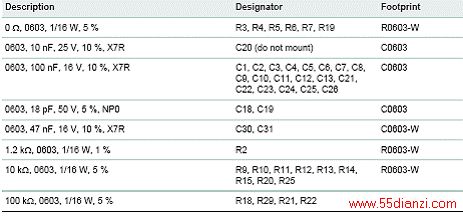
评估板材料清单(BOM):


本文关键字:评估 电子技术,电工技术 - 电子技术

