TI 公司的TPS54260是集成了200毫欧姆高边MOSFET的60V/2.5A降压稳压器, 电流模式控制简化了外部补偿和提供了方便选择元件.输入电压从3.5V到60V,工作静态电流138uA,关断电流1.3uA,开关频率100kHz到2.5MHz.主要应用在12V,24V和48V工业与通信低压电源,GSM和GPRS模块电源.本文介绍了TPS54260主要特性, 功能方框图, 输出3.3V和4.2V设计案例, 反向和分裂电源电路图,以及采用TPS54260开发的GSM/GPRS电源电路和材料清单, TPS54260EVM-597评估模块的性能指标,电路图和材料清单(BOM).
The TPS54260 device is a 60V, 2.5A, step down regulator with an integrated high side MOSFET. Current mode control provides simple external compensation and flexible component selection. A low ripple pulse skip mode reduces the no load, regulated output supply current to 138mA. Using the enable pin, shutdown supply current is reduced to 1.3mA, when the enable pin is low.
Under voltage lockout is internally set at 2.5V, but can be increased using the enable pin. The output voltage startup ramp is controlled by the slow start pin that can also be configured for sequencing/tracking. An open drain power good signal indicates the output is within 94% to 107% of its nominal voltage.
A wide switching frequency range allows efficiency and external component size to be optimized. Frequency fold back and thermal shutdown protects the part during an overload condition. The TPS54260 is available in 10 pin thermally enhanced MSOP Power Pad™ package.
TPS54260主要特性:
3.5V to 60V Input Voltage Range
200-m![]() High-Side MOSFET
High-Side MOSFET
High Efficiency at Light Loads with a Pulse Skipping Eco-Mode™
138µA Operating Quiescent Current
1.3µA Shutdown Current
100kHz to 2.5MHz Switching Frequency
Synchronizes to External Clock
Adjustable Slow Start/Sequencing
UV and OV Power Good Output
Adjustable UVLO Voltage and Hysteresis
0.8-V Internal Voltage Reference
MSOP10 Package With PowerPAD™
Supported by SwitcherPro™ Software Tool
TPS54260应用:
12-V, 24-V and 48-V Industrial and Commercial Low Power Systems
GSM, GPRS Modules in Fleet Management, E-Meters, and Security Systems
图1.TPS54260功能方框图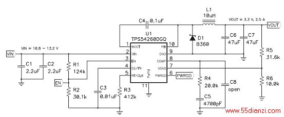
图2.TPS54260输出3.3V设计案例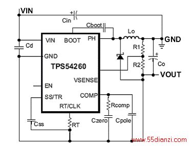
图2.TPS54260反向电源电路图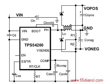
图3.TPS54260分裂电源电路图
图4.采用TPS54260的12V到3.8V的GSM电源电路图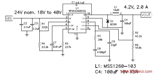
图5.采用TPS54260的24V到4.2V的GSM电源电路图
采用TPS54260开发GSM/GPRS电源
The input voltage supply for the GSM/GPRS module can be from 3.2 V to 4.5 V, with an average power supply current requirement of 400 mA to ~1 A. The power supply must also be able to sustain transmission pulses of 2 A to 3 A, thus considerations for excellent load regulation and low-ripple needs to be taken into account, simultaneously ensuring a highly efficient design.
The average current consumption depends upon the class supported by the module. The most common GPRS classes are Class 8, Class 10 and Class 12. Higher the GPRS class, the faster the data transfer rates and correspondingly it requires more number of timeslots for transmission. Class 8 uses 4 Rx and 1 Tx slot, Class 10 uses 3 Rx and 2 Tx slots and Class 12 uses 1 Rx and 4 Tx slots.
Thus, a GSM/GPRS Module transmits either 1/2/3 time slot(s) of 577us during a 4.6ms period, and receives or remains idle for the rest 4.0ms/3.4ms/2.3ms time depending upon whether it is GSM/GPRS Class 8, Class 10 or Class 12 module. Taking 3 A as the amplitude of transmission bursts, this leads to an average current consumption of about 400mA incase of Class 8 to ~ 1 A in case of Class 12. A power supply design for a GSM/GPRS module should be able to deliver this average current, and also handle intermittent transmission bursts with high current consumption.
GSM/GPRS电源系统参数:

图6. 3.8V输出TPS54260设计案例-1
设计案例-1材料清单(BOM):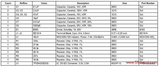
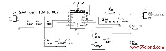
图7. 4.2输出TPS54260设计案例-2
设计案例-2材料清单(BOM):
TPS54260EVM-597 2.5-A, SWIFT™ 稳压器评估模块
TPS54260EVM-597性能指标: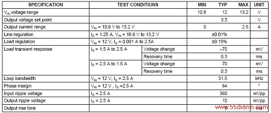
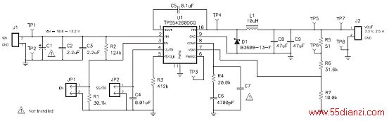
图8.TPS54260EVM-597电路图
TPS54260EVM-597材料清单(BOM):