Freescale ��˾��MCF51CN�ǵͳɱ����ĸ�����32λ��̫��MCU,����32λColdFire V1 CPU,����10/100 BASE-T/TX������̫��������(FEC),�����ⲿ�����շ���(PHY)��ý������ӿ�(MII)ʵ����ҵ��ҵӦ�õ���̫�������Լ�����ⲿ���߽ӿ�. Ŀ��Ӧ���ڽ��������,�����������ҵ����,ҽ�Ƽ��Ӻ�����,POS�Լ���ȫ�뽨������ϵͳ.���Ľ���MCF51CN��Ҫ����,����ͼ,�Լ�TWR-MCF51CN�������·ͼ.
MCF51CN Ethernet MCUs are low-cost, low-power, high-performance 32-bit devices designed for developers who want to add Ethernet connectivity to their commercial and industrial applications.
The MCF51CN128 device is a low-cost, low-power, high-performance 32-bit ColdFire V1 microcontroller (MCU) featuring 10/100 BASE-T/TX fast ethernet controller (FEC), media independent interface (MII) to connect an external physical transceiver (PHY), and multi-function external bus interface.
MCF51CN128 also has multiple communication interfaces for various ethernet gateway applications. MCF51CN128 is the first ColdFire V1 device to incorporate ethernet and external bus interface along with new features to minimize power consumption and increase functionality in low-power modes.
MCF51CN��Ҫ����:
The MCF51CN128 features the following functional units:
• 32-bit ColdFire V1 Central Processing Unit (CPU)
�C Up to 50.33 MHz ColdFire CPU from 3.6 V to 3.0 V, up to 40 MHz CPU from 3.0 V to 2.1 V, and up to 20 MHz CPU from 2.1 V to 1.8 V across temperature range of �C40��to 85��
�C Provides 0.94 Dhrystone 2.1 MIPS per MHz performance when running from internal RAM (0.76 DMIPS/MHz from flash)
�C ColdFire Instruction Set Revision C (ISA_C)
�C Support for up to 45 peripheral interrupt requests and 7 software interrupts
• On-Chip Memory
�C 128 KB Flash, 24 KB RAM
�C Flash read/program/erase over full operating voltage and temperature
�C On-chip memory aliased to create a contiguous memory space with off-chip memory
�C Security circuitry to prevent unauthorized access to Peripherals, RAM, and flash contents
• Ethernet
�C FEC��10/100 BASE-T/TX, bus-mastering fast Ethernet controller with direct memory access (DMA); supports half or full duplex; operation is limited to 3.0 V to 3.6 V
�C MII��media independent interface to connect Ethernet controller to external PHY; includes output clock for external PHY
• External Bus
�C Mini-FlexBus��Multi-function external bus interface; supports up to 1 MB memories, gate-array logic, simple slave device or glueless interfaces to standard chip-selected asynchronous memories
�C Programmable options: access time per chip select, burst and burst-inhibited transfers per chip select, transfer direction, and address setup and hold times
• Power-Saving Modes
�C Two low-power stop modes, one of which allows limited use of some peripherals (ADC, KBI, RTC)
�C Reduced-power wait mode shuts off CPU and allows full use of all peripherals; FEC can remain active and conduct DMA transfers to RAM and assert an interrupt to wake up the CPU upon completion
�C Low-power run and wait modes allow peripherals to run while the voltage regulator is in standby
�C Peripheral clock enable register can disable clocks to unused modules, thereby reducing currents
�C Low-power external oscillator that can be used in stop3 mode to provide accurate clock source to active peripherals
�C Low-power real-time counter for use in run, wait, and stop modes with internal and external clock sources
�C 6 ��s typical wake-up time from stop3 mode
�C Pins and clocks to peripherals not available in smaller packages are automatically disabled for reduced current consumption; no user interaction is needed
• Clock Source Options
�C Oscillator (XOSC) �� Loop-control pierce oscillator; crystal or ceramic resonator range of 31.25 kHz to 38.4 kHz or 1 MHz to 25 MHz
Multi-Purpose Clock Generator (MCG) �� Flexible clock source module with either frequency-locked-loop (FLL) or phase-lock loop (PLL) clock options. FLL can be controlled by internal or external reference and includes precision trimming of internal reference, allowing 0.2% resolution and 2% deviation over temperature and voltage. PLL derives a higher accuracy clock source derived by an external reference
• System Protection
�C Watchdog computer operating properly (COP) reset with option to run from dedicated 1-kHz internal clock source or bus clock
�C Low-voltage detection with reset or interrupt; selectable trip points
�C Illegal opcode and illegal address detection with programmable reset or exception response
�C Flash block protection
• Development Support
�C Single-wire background debug module (BDM) interface; supports same electrical interface used by the S08, 9S12, and 9S12x families debug modules
�C 4 PC plus 2 address (optional data) breakpoint registers with programmable 1- or 2-level trigger response
�C 64-entry processor status and debug data trace buffer with programmable start/stop conditions
• Peripherals
�C ADC��Up to 12 channel, 12-bit resolution; 2.5 ��s conversion time; automatic compare function; 1.7 mV/��C temperature sensor; internal bandgap reference channel; operation in stop3; fully functional from 3.6 V to 1.8 V
�C SCI��Three modules with optional 13-bit break
�C SPI��Two interfaces with full-duplex or single-wire bi-directional; double-buffered transmit and receive; master or slave mode; MSB-first or LSB-first shifting
�C IIC��Two IICs with up to 100 kbps with maxmimum bus loading; multi-master operation; programmable slave address; interrupt-driven byte-by-byte data transfer; supports broadcast mode and 11-bit addressing
�C TPM��Two 3-channel, 16-bit resolution modules; selectable input capture, output compare, or buffered edge- or center-aligned PWM on each channel
�C RTC��8-bit modulus counter with binary- or decimal-based prescaler; external clock source for precise time base, time-of-day, calendar- or task-scheduling functions; free-running on-chip low-power oscillator (1 kHz) for cyclic wake-up without external components; runs in all MCU modes
�C MTIM��Two 8-bit resolution modulo timers with 8-bit prescaler
• Input/Output
�C Up to 70 general-purpose input/output (GPIO) pins, all with pin mux controls to select alternate functions
�C 16 keyboard interrupt (KBI) pins with selectable polarity
�C Hysteresis and configurable pull-up device or input filtering on all input pins; configurable slew rate and drive strength on all output pins 16 Rapid GPIO pins connected to the CPU��s high-speed local bus with set, clear, and toggle functionality (PTD and PTF)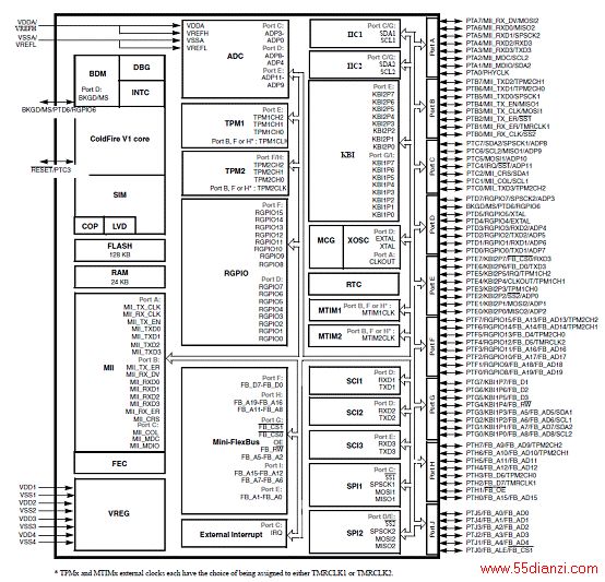
ͼ1.MCF51CN128ϵ�з���ͼ
MCF51CN128ϵ��Ŀ��Ӧ��:
Building control
Industrial operator interfaces
Consumer and industrial appliances
Medical monitoring and instrumentation
Point-of-sale and courier systems
Security and building control systems
TWR-MCF51CN-KIT������
The TWR-MCF51CN-KIT is a low-cost development tool for the MCF51CN128 Ethernet microcontroller. This kit is part of the Freescale Tower System, a modular, reconfigurable development platform that allows designers to get to market faster with packaged evaluation boards, tools and runtime software.
The MCF51CN microcontroller module is designed to be a standalone debug tool and can also be purchased separately from the kit, part number TWR-MCF51CN.
��һƪ��Holtek HT56R66 MUӦ�÷���