一旦系统上电, 数字电位器 新颖地被用做逻辑门功能。
本设计方案描述一个典型的使用PAL(可编程逻辑阵列)、GAL(门逻辑阵列)或CPLD(复杂的可编程逻辑设备)实现相对简单的 非易失性 门功能。为控制 逻辑信号 来阻塞或传输逻辑信号,通常使用逻辑门,如与门。使用门的第二个输入来决定门是阻塞还是传输应用信号。因为逻辑门实现直接布尔操作,它们的操作是没有存储器配合的可组合逻辑。
然而,系统启动后,如果设计经常阻塞或传输信号的门,在非易失性存储器的某些形式下,必须存储“传输/阻塞” 的逻辑状态。两个基本方法用于存储这种逻辑状态。第一个使用微处理器结合非易失性存储器,例如EEPROM。如果系统可以等到微处理器从存储器读出逻辑状态,并应用到硬件管脚,如典型的GPIO口,这种方法是适用的。然而,一些系统需要在上电时就传输/阻塞信号。对那些系统,存储器的读延时是不可接受的。
第二种方法用于没有微处理器或启动时微处理器不能等到存储器读出的系统,在启动时存储逻辑状态的设备可用。为了这个目的,采用PAL、GAL和CPLD设备结合可编程非易失性存储器实现控制功能。然而,这些设备提供更多存储器控制和不需要门的特殊系统。它们的封装也相当大到足以容纳许多逻辑I/O引脚。
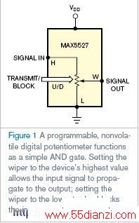
如果不需要非易失性门,考虑使用器件共用在模拟和混合信号系统中:数字电位器(图1)。将电阻线的L端接地,信号由H端接入回路。然后,输出触点短接到地阻塞或连接到输入信号传输。
单板或系统测试期间,通过串行接口为数字电位器编程。一些数字电位器的通讯接口适于这个目的。当选择非易失性数字电位器时,应考虑以下标准:
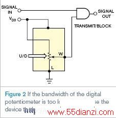
数字电位器的带宽决定信号通过电位器传输的最大数据率。如果这些应用逻辑信号的开关率对使用的电位器过高,可以使用带数字电位器控制传输/阻塞输入的传统高速逻辑门(图2)。
英文原文:
Nonvolatile digital potentiometer gates logIC signal
A novel use for digital potentiometers employs them as a logic gate that functions as soon as the system powers up.
Reinhardt Wagner, Maxim Integrated Products, Ottobrunn, Germany; Edited by Charles H Small and Fran Granville -- EDN, 9/3/2007
This Design Idea describes a simple aLTErnative to a nonvolatile gating function you typically implement using PAL (programmable-array logic), GAL (gate-array logic), or a CPLD (complex-programmable-logic device). To gate a logic signal to bLOCk or transmit it, you usually employ a logic gate, such as an AND gate, and use the gate’s second input to define whether the gate blocks or transmits the applied signal. Because logic gates perform immediate Boolean operations, their operations are combinational and without memory.
A second method, which is useful for systems without a microcontroller or that cannot wait for the microcontroller to read from memory at boot time, stores the logic state in a device that makes it immediately available at power-up. For this purpose, PAL devices, GAL devices, and CPLDs implement the gating function in combination with programmable nonvolatile memory. These devices offer more than gating with memory, however, and may be overspecified for systems that need only a few such gates. Also, their PACkages are relatively large to accommodate the many logic-I/O pins they offer.
If you need only a few nonvolatile gates, consider using a component common in analog- and mixed-signal systems: the digital potentiometer (Figure 1). Ground the L end of the resistor string and route the signal into the H end of the string. Then, the wiper output either shorts to ground for blocking or connects to the input signal for transmission.
You can program the digital potentiometer through its serial interface during board or system test. The up/down interface on some digital potentiometers is suitable for that purpose. When selecting a nonvolatile digital potentiometer, you should consider the following criteria:
The digital potentiometer’s bandwidth determines the maximum data rate for signals transmitted through the potentiometer. If the switching rate of these applied logic signals is too high for the available potentiometers, you can use a conventional, high-speed logic gate with a digital potentiometer controlling the transmit/block input (Figure 2).
英文原文地址: http://www.edn.com/article/CA6470827.html
本文关键字:电位器 数字电位器,单元电路 - 数字电位器