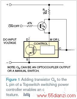
ͼ1 ������M��L���źͿ�������֮���NPN�;����QR
����ͼ2�еĵ�·�ṩһ���¹��ܣ�����ʹ����ʱ�ȿ������Ÿ������ �ӵؿ��� ��������ѹ�����ء��ڻ�е���ص�����£���·����Ҫ�ⲿ��Դʵ��������ܡ��������Ӧ����Ϊ��Ҫ��Topswitch�ĵ�Դ������Ψһ��Դ����·�������M��L���ŵĹ���ѹ��Ƿ��ѹ���ܡ�Ϊ����ͼ2�е�·�Ĺ�����ҪM��L�����ڲ�����ԭ���Ľ��͡���������ӽ�2Vֱ���ĺ�ֵ��ѹԴ���ã���ʹRLS�ṩ���ⲿ��·�������͡�����ѹ��Ƿ��ѹ�����ڲ��������м����50 &mICro;A������30 µA��Ƿ��ѹ����225 µA�Ĺ���ѹ�ͺ������˵��������M��L���ŵĵ�������30 µA����30��50 µA֮��ʱ����ѹ���������Ƿ��ѹ���رա�������M��L���ŵĵ���Ϊ225 µA��ʱ����ѹ��������ڹ���ѹ���رա�������M��L���ŵĵ���Ϊ50��225 µA��ʱ�������ʹ�ܡ�

ͼ2 ΪTopswitchоƬ�Ŀ��ؿ������ӽӵؿ��صĹ��ܵ�·
����ͼ2�е�·�����·�ʽ��������Q1���缫���صĿ��ص�ͨʱ��Q1��Ϊ������ʹ�伫��
��������0.6Vѹ��������RLS�ṩ�ĵ���ͨ��Q1�Ļ����伫����150kΩ�������M��L���š�������ģʽ�£�Topswitch���ɵ�·���й���ѹ��Ƿ��ѹ�ļ��ޡ�Ȼ���������ؽӵ�ʱ��Q1�Ĺ��ܾ��൱���и�����ı��;���ܡ������·���մ���RLS���صĵ�����ΪQ1�ļ��缫������Q1��С������������4 µA��ͨ��150kΩ��������M��L���š���ͼ2����ֵ��������Q1������С��������450V�����ѹ��ʱ��������ҲС��3.8µA����ˣ�3.8µA��7.8µA����M��L���š����ֵ͵������� “fools”���ź���ѹ����“thinking”�������ѹ����Ƿ��ѹ״̬����ʹ��ѹ������رա�
������������и���ѹ�����Դ���ڣ��ý��м�С�������õļ��缫��·���ش���S1�����ң�ؿ����������������һ��������������������Ӧ����Q1�ļ��缫���ش���������ܣ�����������������������������ֱ��2V���ر���ѹ����ͼ2��ѡ����M����Ҳ�����������ĵ��ڡ�
����Ӣ��ԭ�ģ�
����Add a grounded-switch feature for Topswitch on/off control
����Adding a couple of components to the control PIN of a Topswitch switching regulator enables on/off control.
����Robert N Buono, Aeolian Audio LLC, BloomfiELD, NJ; Edited by Charles H Small and Fran Granville -- EDN, 6/21/2007
����The Power Integrations Topswitch family of integrated flyback-regulator ICs provides exceptional performance in small, low-pin-count PACkages. For the lowest-pin-count packages, the multifunction, or M, pin serves multiple purposes, including on/off control and undervoltage- and overvoltage-input detection. Other package types include an L pin, which also provides this function. The application notes and data sheets show how to implement the various features available at these pins. For example, to allow remote on/off control and still preserve undervoltage and overvoltage functions, the application drawings show an NPN transistor, QR, which connects between the M or L pin and the Control pin (Figure 1). To turn off the regulator, QR must be biased on. To achieve this goal requires a base voltage of 2.6V dc or greater.
����The circuit in Figure 2 provides a new feature that allows you to switch the regulator on or off usi ng a grounded switch that is sometimes more convenient to implement than a switch that references to the Control PIN. In the case of a mechanICal switch, this circuit would require no external power to implement this function. This feature is important in applications in which the Topswitch power supply is the only source of power. This circuit does not disturb the functioning of the undervoltage and overvoltage functions of the M or L pin. To understand the functioning of the circuit in Figure 2 requires an explanation of the internal workings of the M or L pin. This pin acts as a constant voltage source at approximately 2V dc and sinks current from the external circuit, which RLS supplies. The internal current-sense thresholds for undervoltage and overvoltage detection are roughly 50 µA with 30 µA of hysteresis for undervoltage and 225 µA for overvoltage. That is, when the current into the M or L pin is less than 20 µA, or 50�C30 µA, the regulator output switches off because of undervoltage. When the current into the M or L pin exceeds 225 µA, the regulator output switches off because of overvoltage. When the current into the M or L pin is 50 to 225 µA, the output is enabLED.
����The circuit of Figure 2 works as follows: When the switch in the collector lead of Q1 is open, Q1 functions as a simple diode with a 0.6V drop from EMItter to base. All the current that RLS supplies flows into the M or L pin through the base-emitter junction of Q1 and the 150-k�� resistor. In this mode, the Topswitch IC senses the undervoltage and overvoltage thresholds. However, when the switch to ground closes, Q1 functions as a nonsaturated transistor with high gain. The circuit SIPhons off most of the current through RLS to ground as the collector current of Q1. Only a small base current from Q1 plus 4 µA through the 150-k�� resistor flows into the M or L pin. For the values in Figure 2, this base current is less than 3.8 µA, even when Q1 has minimum gain and input voltage is at a maximum of 450V dc. Therefore, 3.8+4 µA, or 7.8 µA, flows into the M or L pin. This low current flowing into the pin ��fools�� the regulator into ��thinking�� that the input voltage is undervoltage, and the regulator output switches off.
����If another voltage or current source is present, you could replace S1 with an open-collector switch that sinks current only. If the remote on/off driver CAN source and sink current, as the output of a logic gate can, then you should insert a diode in the collector lead of Q1, and the driver must drive the cathode of that diode above 2V dc to turn off the regulator (optional in Figure 2). The M pin also allows current-limit-threshold adjustment.
����Ӣ��ԭ�ĵ�ַ�� http://www.edn.com/index.asp?layout=article&articleid=CA6451247&sPACedesc=DesignIdeas&taxid=10577&industryid=44217
���Ĺؼ��֣����� Ԫ�����ص㼰Ӧ����Ԫ�������� - Ԫ�����ص㼰Ӧ��