随着3D技术的演化以及应用中通孔尺寸和节距的缩小,叠层中每层的厚度也很有可能会减小。截至目前的测试表明,即使将硅片厚度减到5μm以下,电路性能也不会恶化。因此,很有可能的是,可制造性而非电学性能将成为未来的限制因素。此外,当考虑先通孔或后通孔方案时,厚度变得很重要。后者在硅刻蚀开始之前,需要先额外刻蚀厚度超过6μm的后道介质层。对于薄硅层来说,这将对刻蚀的深宽比造成很大影响。
诸如CMOS图像传感器、存储器、逻辑电路上存储器之类3D应用,在未来2-3代内都不会需要使用大于5的深宽比。在TSV尺寸降到约1μm甚至更小之前,我们将不会看到深宽比达到10-20范围。
铜通孔中,TiN粘附/阻挡层和铜种子层都通过溅射来沉积。然而,要实现高深宽比(AR>4:1)的台阶覆盖,传统的PVD直流磁控技术效果并不令人满意。基于离子化金属等离子体(IMP)的PVD技术可实现侧壁和通孔底部铜种子层的均匀沉积。由于沉积原子的方向性以及从通孔底部到侧壁溅射材料过程中离子轰击的使用,IMP提供更好的台阶覆盖性和阻挡层/种子层均匀性。
晶圆键合 技术选择
针对3D集成而考察的晶圆键合技术包括:
高分子粘结键合
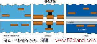
由于特征尺寸的限制,图6所示全部键合技术都需要特别光滑、平整和洁净的表面。尽管所有这些技术看起来都可行,但有一种趋势是转向使用金属-金属键合技术,因为这种技术可以同时实现机械和电学的接触界面。铜-铜键合直接铜键合工艺需要到在350-400℃温度下施加压力超过30分钟,接着在350-400℃下的氮气气氛退火30-60分钟。这一工艺需要高度抛光的铜表面并保持很高的洁净度。像EVGroup(奥地利St.Florian/Inn)和SUSSMICroTec(佛蒙特州,Waterbury)等厂商提供的商业化工具,需要在单个对准工具上装有多个键合头,才能得到可接受的产能。一种像Ziptronix(北卡罗来纳州,Morrisville)报道的称作直接键合互连(DBI)的工艺,据说可以大大提高这一产能。这种技术使用金属对TSV进行封帽,之后采用氧化物、金属同步CMP进行平坦化,经过专利保护的表面处理技术,可使用标准的键合/对准机在大气环境下1-2分钟内实现芯片或者晶圆的键合。在350℃温度下施加压力,在低CoO键合操作下可以获得了单一的金属界面。
3D应用
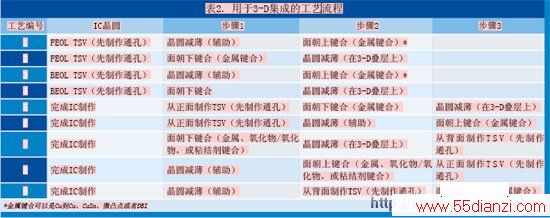
表2总结了九种不同的3D集成工艺流程,都对应从晶圆工艺一直到键合。
本文的第二部分将重点对3D技术商业化过程中的重点参与者进行介绍。将会介绍3D集成的可能应用领域,比如存储器与逻辑电路、闪存叠层以及其他的一些重点方向。
References
1. A. Braun, “Low-k Bursts Into the Mainstream…Incrementally,” SEMIconductor International, May 2005, p. 41.
2. K. Saraswat, “3D IC's: Motivation, Performance Analysis and Technology,” 3D Architectures for Semiconductor Integration & PACkaging, Phoenix, June 2005.
3. S. Vitkavage and K. Monnig, “3D Interconnects and the IRTS RoaDMAp”, Proc. 3D Architecture for Semiconductor Integration and Packaging Conf., Phoenix, 2005.
4. J.A. Davis et al., “Interconenct Limits on Gigascale Integration in the 21st Century”, Proc. IEEE, Vol. 89, 2001, p. 305.
5. P. Garrou, “3D Integration Invades Whitefish Montana,” Perspectives From the Leading Edge, Sept. 7, 2007.
6. P. Morrow et al., “Design and Fabrication of 3D Microprocessors,” MRS Proc., Vol. 970, Enabling Technologies for 3D Integration, C.Bower, P. Garrou, P. Ramm, K. Takahashi Eds., 2007, p. 91.
7. P. Garrou, “Future ICs Go Vertical,” Semiconductor International, February 2005, p. SP10.
8. P. Garrou, “3D IC Integration: Evolution or Revolution?”, Perspectives From the Leading Edge, March 16, 2008.
9. P. Garrou, “ASET Drives 3D Integration Workshop in Tokyo,” Perspectives From the Leading Edge, June 21, 2008.
10. P. Garrou, “Going Vertical in Whitefish,” Sept. 9, 2007; “High Throughput Laser Drilling for 3D IC TSV,” Feb. 17, 2008, Perspectives From the Leading Edge.
11. P. Garrou, “3D EQUIPment & Materials Vendors Consortium,” Perspectives From the Leading Edge, Aug. 26, 2007.
12. P. Garrou, “3D Practitioners Assemble at Fort McDowell,” Perspectives From the Leading Edge, March 23, 2008.
13. P. Garrou, “NXP Proposes Passive Integration in 3D IC Stacks,” Perspectives From the Leading Edge, April 13, 2008.
14. P. Garrou, “More 3D Integration at ECTC 2008,” Perspectives From the Leading Edge, June 28, 2008.
15. P. Garrou, “If It's Thursday It Must Be San Jose,” Perspectives From the Leading Edge, June 8, 2008.
16. D.M. Jang et al., 57th EleCTRonic Component Tech. Conf. 2007, p. 847.
17. P. Garrou, “3D Road Tour Continued,” Perspectives From the Leading Edge, May 28, 2008.
18. Handbook of 3D Integration, P. Garrou, P. Ramm & C. Bower Eds., Wiley-VCH.