NS LM5001 RD-171双电源参考设计方案
NS LM5001 RD-171双电源参考设计方案
点击数:7676 次 录入时间:03-04 11:37:01 整理:http://www.55dianzi.com 电工文摘
NS 公司的RD-171双电源参考设计方案采用LM5001器件,具有非常低噪音的差分电源,即可产生相互绝缘的+5V和-5V电源(也可是更高电压或更低电压),总功率为2.5W,电流0.25A.设计采用双面FR4 PCB,完全绝缘的输出,隔离电压大于500V,噪音小于20 mV P-P,工作频率600kHz,同时PCB的占位面积非常小.而LM5001是全集成的反激式稳压器,具有电流模式控制的所有性能.本文首先介绍了LM5001的主要特性,方框图, LM5001升压稳压器应用电路图, 非绝缘和绝缘反激电路图, 24V 和12V SEPIC电路图.接着介绍了RD-171参考设计的主要特性,框图, 参考设计电路图和所用材料清单(BOM).
+/- 5V Isolated, Low Noise Split Rail Generator (0.25A, 2.5W total)

NS RD-171参考设计外形图
The LM5001 high voltage switch mode regulator features all of the functions necessary to implement efficient high voltage Boost, Flyback, SEPIC and Forward converters, using few external components. This easy to use regulator integrates a 75 Volt N-Channel MOSFET with a 1 Amp peak current limit.
Current mode control provides inherently simple loop compensation and line-voltage feed-forward for superior rejection of input transients. The switching frequency is set with a single resistor and is programmable up to 1.5MHz. The oscillator can also be synchronized to an external clock. Additional protection features include: current limit, thermal shutdown, under-voltage lockout and remote shutdown capability. The device is available in both SO-8 and LLP-8 packages.
LM5001主要特性:
■Integrated 75 volt N-Channel MOSFET
■Ultra-wide input voltage range from 3.1V to 75V
■Integrated high voltage bias regulator
■Adjustable output voltage
■1.5% output voltage accuracy
■Current mode control with selectable compensation
■Wide bandwidth error amplifier
■Integrated current sensing and limiting
■Integrated slope compensation
■85% maximum duty cycle limit
■Single resistor oscillator programming
■Oscillator synchronization capability
■Enable / Undervoltage Lockout (UVLO) pin
■Thermal shutdown
Packages
■SO-8
■LLP-8 (4mm x 4mm)

图1.LM5001方框图
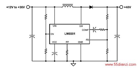
图2.LM5001升压稳压器应用电路图
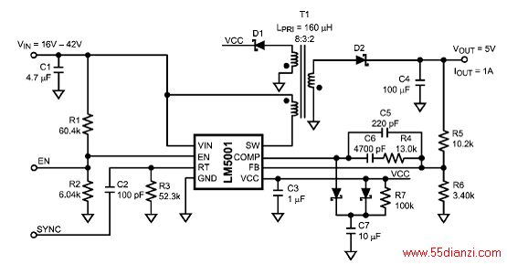
图3.LM5001非绝缘反激电路图

图4.LM5001绝缘式反激电路图

图5.LM5001升压电路图
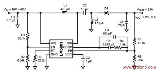
图6.LM5001 24V SEPIC电路图
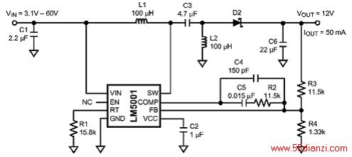
图7.LM5001 12V SEPIC电路图
RD-171参考设计
A very low noise differential power supply for split rail systems requiring low noise +5V and -5V (higher or lower voltage is possible). This design is fully isolated and capable of floating to over 500V differential from Vin to Vout (higher is possible).
The LM5001 IC is a fully integrated flyback regulator which performs all of the current mode control for tight regulation and transient response. The design is small and uses only one side of a double sided FR4 PCB for components. Smaller IC packages are available so the layout can be further optimized.
This design provides very low noise bias rails for ground referenced analog circuitry (under 20 mV p-p total noise up to 1GHz). The design utilizes a very small size PCB footprint.
This approach is ideal for many applications including low noise cable drivers, medical electronics, high fidelity low power audio, and other sensitive circuitry that can benefit from
very low noise split rail biasing. Input to output isolation is employed for those applications where the input and output voltages might be at different potentials or when the input
voltage travels across cabling which might pickup noise. The floating outputs avoid unwanted ground currents and the potential for additional noise pickup. For those that do not require isolation they can remove the feedback isolation section of the design and use a simple resistor divider for setting the feedback voltage.
RD-171参考设计主要特性:
■Very Low Noise, <2 0 mV P-P
■Fully Isolated Outputs, > 500V
■Small Size
■Wide Input Range > 10V - 30V
■Double sided PCB
■600 KHz Operation
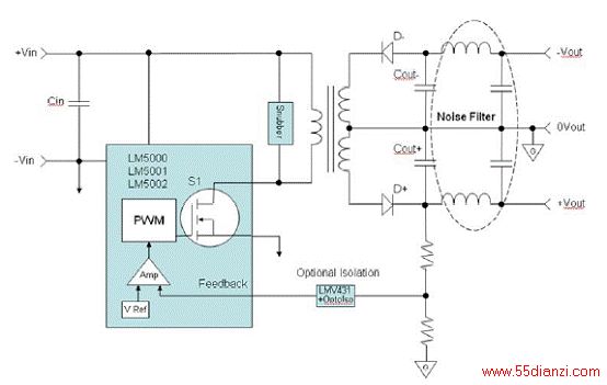
图8.RD-171参考设计框图
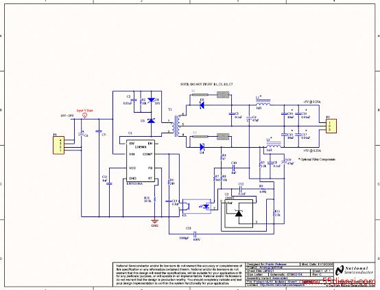
图9.RD-171参考设计电路图
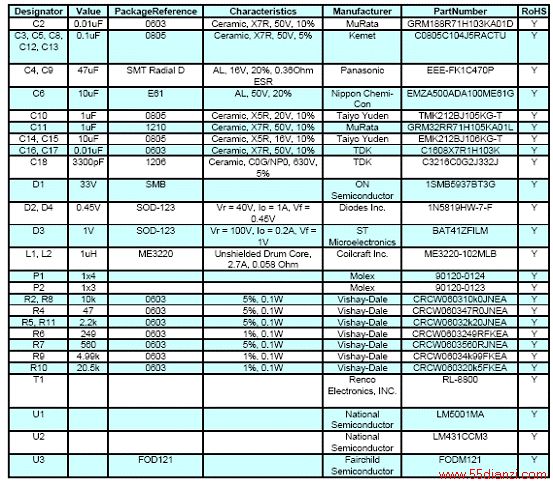
RD-171参考设计材料清单(BOM):
本文关键字:电源 电工文摘,电工技术 - 电工文摘