For write operations, the serial control word is followed by a 16-bit data word and is latched internally on rising SCLK edges.
For read operations, a bus turn-around of half a cycle is followed by a 16-bit data word shifted out on rising SCLK edges and is clocked into the system controller on falling SCLK edges. The transfer ends on the rising SCLK edge after SEN is set high. Note that 26 SCLK cycles are required for a transfer, however, SCLK may run continuously.
For details on timing specifications and diagrams, refer to Table 6, ��3-Wire Control Interface Characteristics,�� on page 8, Figure 3, ��3-Wire Control Interface Write Timing Parameters,�� on page 8, and Figure 4, ��3-Wire Control Interface Read Timing Parameters,�� on page 9.
2-wire Control Interface
For two-wire operation, the SCLK and SDIO pins function in open-drain mode (pull-down only) and must be pulled up by an external device. A transfer begins with the START condition (falling edge of SDIO while SCLK is high). The control word is latched internally on rising SCLK edges and is eight bits in length, comprised of a seven bit device address equal to 0010000b and a read/write bit (write = 0 and read = 1).
The device acknowledges the address by driving SDIO low after the next falling SCLK edge, for 1 cycle. For write operations, the device acknowledge is followed by an eight bit data word latched internally on rising edges of SCLK. The device acknowledges each byte of data written by driving SDIO low after the next falling SCLK edge, for 1 cycle. An internal address counter automatically increments to allow continuous data byte writes, starting with the upper byte of register 02h, followed by the lower byte of register 02h, and onward until the lower byte of the last register is reached. The internal address counter then automatically wraps around to the upper byte of register 00h and proceeds from there until continuous writes end. Data transfer ends with the STOP condition (rising edge of SDIO while SCLK is high). After every STOP condition, the internal address counter is reset.
��Ҫ����:
This data sheet applies to Si4702/03-C Firmware 19 and greater
Worldwide FM band support (76�C108 MHz)
Digital low-IF receiver
Frequency synthesizer with integrated VCO
Seek tuning
Automatic frequency control (AFC)
Automatic gain control (AGC)
Excellent overload immunity
Signal strength measurement
Programmable de-emphasis (50/75 ��s)
Adaptive noise suppression
Volume control
Line-level analog output
32.768 kHz reference clock
2-wire and 3-wire control interface
2.7 to 5.5 V supply voltage
Integrated LDO regulator allows direct connection to battery
3 x 3 mm 20-pin QFN package
Pb-free/RoHS compliant
RDS/RBDS Processor (Si4703)
Integrated crystal oscillator
Ӧ��:
Cellular handsets
MP3 players
Portable radios
USB FM radio
PDAs
Notebook PCs
Portable navigation
Consumer electronics
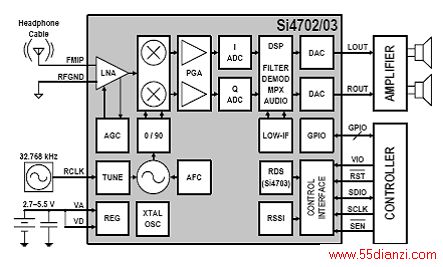
ͼ1.Si4702/03C���ܷ���ͼ
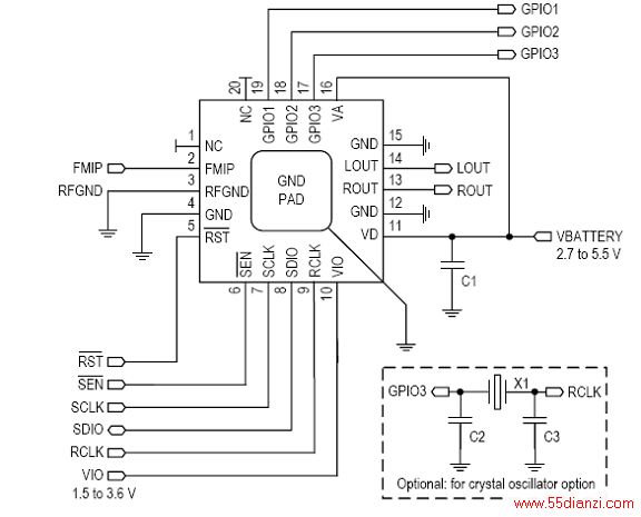
ͼ2. Si4702/03C����Ӧ�õ�·

��1.����Ӧ�õ�·�в����嵥(BOM)
��һҳ [1] [2] [3]
���Ĺؼ��֣�������ϵ��ʽ���Ӽ������繤���� - ���Ӽ���